


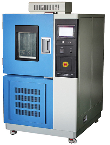
Climate Chambers for MIL-STD-750E: Department of Defense Test Method Standard Test Methods for Semiconductor Devices
Welcome to our website:http://www.lenpure.com/
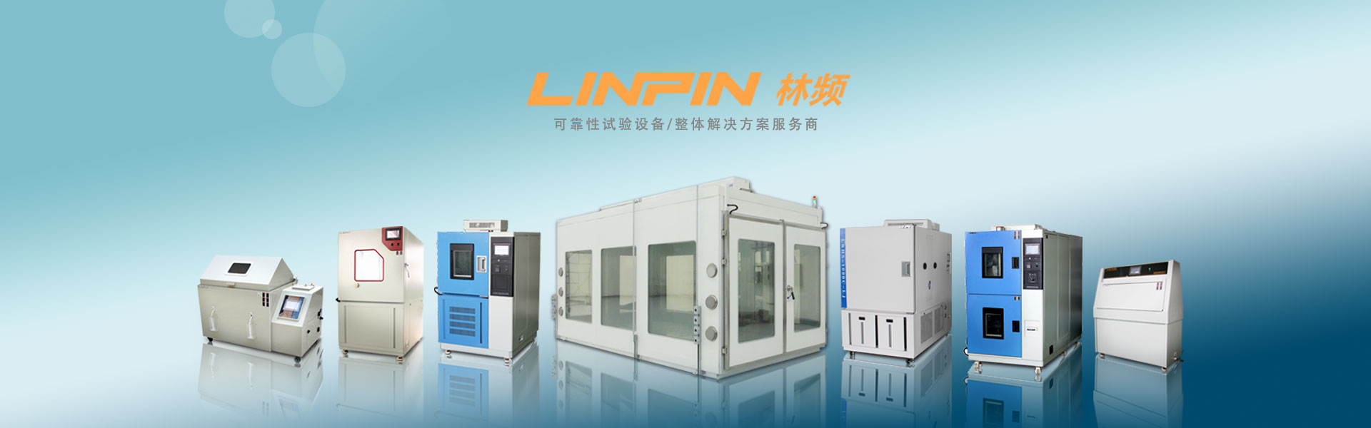
Shanghai Linpin Instrument Stock Co., Ltd China is a leading environmental test chambers manufacturer providing various kinds of climatic chambers for numerous industries. Our factory are located in Shanghai China; Aiming to provide customers with best products as well as service, Lenpure does it utmost to pursue perfection during every process.
From design to after-sales troubleshooting with elite engineers team,the one-stop solution and service bring partners cost-saving,time-saving and energy-saving cooperation relations.
Basic Information of LENPURE:
Registered capital 8.64 millions USD
There are 8.64 millions USD in the appointed bank account,under monitoring of government, means LENPURE pay ability to related business partners once company go bankrupt. By now in China market of environmental test chamber,even Espec &Weiss,they are far behind us. Right is the business license of LENPURE ,with the Registered capital in RMB 51.8 million.
30000 square meters owned workshop & office area
The land is one of LENPURE ’s property ,and the buildings & workshops
were all built on our own design.This means we were doing very will in our business,
Lenpure win the good reputation & get a have powerful economic strength to running better.
Location
Headquarters: Shanghai
Branches: Total 15 Branches, located in Beijing,Shenzhen, Shenyang,etc.
Most of medium-sized cities, all big cities in China,we all have office to provide pre and after sale service.
Main Market
America,Europe.Asia, Oceania, etc.
On-site Installation & always reply in time for after-sale service.
1. SCOPE
1.1 Purpose
This standard establishes uniform methods for testing semiconductor devices, including basic environmental tests to determine resistance to deleterious effects of natural elements and conditions surrounding military operations, and physical and electrical tests. For the purpose of this standard, the term "devices" includes such items as transistors, diodes, voltage regulators, rectifiers, tunnel diodes, and other related parts. This standard is intended to apply only to semiconductor devices. The test methods described herein have been prepared to serve several purposes:
A. To specify suitable conditions obtainable in the laboratory that give test results equivalent to the actual service conditions existing in the field, and to obtain reproducibility of the results of tests. The tests described herein are not to be interpreted as an exact and conclusive representation of actual service operation in any one geographic location, since it is known that the only true test for operation in a specific location is an actual service test at that point.
B. To describe in one standard all of the test methods of a similar character which now appear in the various joint-services semiconductor device specifications. so that these methods may be kept uniform and thus result in conservation of equipment, man-hours, and testing facilities. In achieving this objective, it is necessary to make each of the general tests adaptable to a broad range of devices.
C. The test methods described herein for environmental, physical, and electrical testing of devices shall also apply, when applicable, to parts not covered by an approved military sheet-form standard, specification sheet, or drawing.
1.2 Nurnbering system.
The test methods are designated by numbers assigned in accordance with the following system
1.2.1 Classification of tests
The tests are divided into five areas. Test methods numbered 1001 to 1999 inclusive cover environmental tests; those numbered 2001 to 2999 inclusive, cover mechanical- characteristics tests.Electrical- characteristics tests are covered in two groups; 3001 to 3999 inclusive, covers tests for transistors and 4001 to 4999 inclusive, covers tests for diodes. Test methods numbered 5000 to 5999 inclusive, are for high reliability space applications.
1.2.2 Revisions
Revisions are numbered consecutively using a period to separate the test method number and the revision number. For example, 4001.1 is the first revision of test method 4001.
1.3 Method of reference
When applicable, test methods contained herein shall be referenced in the individual specification by specifying the method number of this standard, and the details required in the summary of the applicable method. To avoid the necessity for changing specifications that refer to this standard, the revision number should not be used when referencing test methods. (For example: use 4001, not 4001.1.)
2.APPLICABLE DOCUMENTS
2.1 General. The documents listed in this section are specified in sections 3. 4. or 5 of this standard. This section does not include documents cited in other sections of this standard or recommended for additional information or as examples. While every effort has been made to ensure the completeness of this list, document users are cautioned hat they must meet all specified requirements documents cited in sections 3. 4. or 5 of this specification. whether on not they are listed.
4. GENERAL REQUIREMENTS
4.1 Test conditions
Unless otherwise specified herein or in the individual specification, all measurements and tests shall be made at thermal equilibrium at an ambient temperature of 25°C ±3°C and at ambient atmospheric pressure and relative humidity and the specified test condition C (at environmentally elevated and reduced temperatures) shall have a tolerance of ±3 percent or +30C, whichever is greater. Whenever these conditions must be closely controlled in order to obtain reproducible results. the referee conditions shall be as follows: Temperature 25°C ±1 C, relative humidity 50 ±5 percent, and atmospheric pressure from 650 to 800 millimeters of mercury.Unless otherwise specified in the detail test method. for mechanical test methods, 2000 series, the ambient.may be 25°C ±10°C.
4.2 Orientations
X is the orientation of a device with the main axis of the device nornal to the direction of the accelerating force, and the maior cross section parallel to the direction of the accelerating force.
Y is the orientation of a device with the main axis of the device parallel to the direction of the accelerating force.and the principal base toward (Y1), or away from (Y2), the point of application of the accelerating force.
Z is the orientation of a device with the main axis and the major cross section of the device normal to the direction of the accelerating force. Z is 90 degrees of X.
NOTE: For case configurations. other than those shown on figures 1 and 2. the orientation of the device shall be as specified in the individual specification.
4.3 General precautions
The following precautions shall be observed in testing the devices.
4.3.1 Transients Devices shall not he subjected to conditions in which transients cause the rating to he exceeded.
4.3.2 Test conditions for electrical measurements
Unless otherwise required for a specified test method semiconductor devices should not be subjected to any condition that will cause any maximum rating of the device to be exceeded. The precautions should include limits on maximum instantaneous currents and applied voltages. High series resistances (constant current supplies) and low capacitances are usually required. If low cutoff, or reverse current devices are to be measured; for example, nanoampere units, care should be taken to ensure that parasitic, circuit currents or external leakage currents are small, compared with the cutoff or reverse current of the device to be measured.
4.3.2.1 Steady-state dc measurements (method 4000)
Unless otherwise specified, all steady-state dc parameters are defined using.
4.3.2.2 Pulse measurements (method 4000)
When device static or dynamic parameters are measured under pulsed conditions, in order to avoid measurement errors introduced by device heating during the measurement period. the following items should be covered in the performance specification sheet:
A.The statement "pulsed test shall be placed by the test specified.
B.Unless otherwise specified, the pulse time (t.) shall be s10 milliseconds and the duty cycle shall be a maximum of 2 percent; within this limit the pulse must be long enough to be compatible with test equipment capability and the accuracy required, and short enough to avoid heating.
4.3.3 Test circuits
The circuits shown are given as examples which may be used for the measurements. They are not necessarily the only circuits which can be used but the manufacturer shall demonstrate to the Govemment that other circuits which they may desire to use will give results within the desired accuracy of measurement. Circuits are shown for PNP transistors in one circuit configuration only. They may readily be adapted for NPN devices and for other circuit configurations.
4.3.3.1 Test method variation
Variation from the specified test methods used to verify the electrical parameters are allowed provided that it is demonstrated to the preparing activity or their agent that such variations in no way relax.the requirements of this specification and that they are approved before testing is performed. For proposed test variations, a test method comparative error analysis shall be made available for checking by the preparing activity on their agent.
4.3.4 Soldering
Adequate precautions shall be taken to avoid damage to the device during soldering required for tests.
4.3.5 Order of connection of leads
Care should be taken when connecting a semiconductor device to a power source. The common terminal shall be connected first.
4.3.6 Radiation precautions
Due precautions shall be used in storing or testing semiconductor devices in.substantial fields of X-rays, neutrons, or other energy particles.
4.3.7 Handling precautions
4.3.7.1 UHF and microwave devices. Handling precautions for UHF and microwave devices shall be as follows:
a. Ground all equipment
B. Make hand contact to the equipment while holding the base end and maintain hand contact with the equipment until the device is in place.
C.Where applicable, keep devices in metal shields until they are inserted in the equipment or until necessary to remove for test.
4.3.7.2 Electrostatic discharge sensitive devices. Handling precautions shall be observed in accordance with MIL-HDBK-263 during testing of Electrostatic Discharge Sensitive (ESDS) devices. The area where ESDS device tests are performed shall meet the requirements of an ESD Protected Area of MIL STD-1686.
4.4 Continuity verification of burn-in and life tests
The test setup shall be monitored at the test temperature initially and at the conclusion of the test to establish that all devices are being stressed to the specified requirements. The following is the minimum acceptable monitoring procedure:
A.Device sockets. Initially and at least each 6 months thereafter, each test board or tray shall be checked to verify continuity to connector points to assure that the correct voltage bias will be applied. Except for this initial and periodic verification, each device or device socket does not have to be checked; however random sampling techniques shall be applied prior to each time a board is used and shall be adequate to assure that there are correct and continuous electrical connections to the Device under test (DUT).
B.Connectors to test boards or trays. After the test boards are loaded with devices, inserted into the system and brought up to the specified operating conditions, each required test voltage and signal condition shall be verified in at least one location on each test board or tray so as to assure electrical continuity and the correct application of specified electrical stresses for each connection or contact pair used in the applicable test configuration. The system may be opened for a maximum of 10 minutes.
C.At the conclusion of the test period, prior to removal of devices from temperature and bias conditions, the voltage and signal condition verification of 4.4b shall be repeated.
D.For class S devices. each test board or tray and each test socket shall be verified prior to test to assure that.the specified bias conditions are applied to each device. This may be accomplished by verifying the device functional response at each device output(s) or by performing a socket verification on each socket prior to loading. An approved alternate procedure may be used.
4.4.1 Bias interruption
Where failures or open contacts occur which result in removal of the required bias stresses for any period of the required bias duration, the bias time shall be extended to assure actual exposure for the total minimum specified test duration. Any loss(es) or interruption(s) of bias in excess of 10 minutes total duration while the chamber is at temperature during the final 8 hours of bum-in shall require extension of the bias duration for an uninterrupted 8 hours minimum, after the last bias interruption.
4.5 Requirements for High Temperature Reverse Bias (HTRB) and bum-in.
A.The temperature of +20C minimum is the ambient air temperature to which all devices should be exposed during power screening where room ambient is specified.
B.An increase in effective ambient temperature from cumulative induced power to DUTs shall not result in.device junction temperature exceeding maximum ratings.
C.Ambient temperature shall not be measured in the convection current (above) or downstream (Fan Air) of DUTs.
D.Moving air greater than 30 CFM (natural convection) may be allowed for the purpose of temperature equalization within high device density burn-in racks.
E.High velocity or cooled air shall not be used for the purpose of increasing device ratings.
F.Power up of burn-in racks may occur when ambient is less than specified. When thermal equilibrium has been reached. or five hours maximum has occurred, the ambient shall be at the specified value. Time accrued prior to reaching specified ambient shall not be chargeable to the life test duration.
G.If the ambient, at or beyond the five hour point is not the specified value,a nonconformance shall exist requiring corrective action.
H.Time is not chargeable during the period when specified conditions are not maintained. If device maximum ratings (if life test, finish the test and use for credit; if shippable, use this criteria) are exceeded and the manufacturer intends to submit the lot affected, the product on test shall be evaluated by re-starting the urn-in or HTRB from zero hours at the specified temperature and verifying that the end-point failure rate is typical for this product type from a review of established records.
I.Chamber temperature for HTRB and burn-in shall be controlled to t3 percent of the specified value (unless otherwise specified in 4.1.1). This temperature shall be maintained within the chamber. Forced air may be used to equalize temperature within the chamber but shall not be used as a coolant to increase device power capability.
4.6 Bias requirements
A.Bias errors at the power supply source caused by changing power supply loads during temperature transitions shall not exceed +5 percent of that specified value.
B.Bias values at the source, during stabilized conditions. shall not exceed t3 percent of the specified value.
C.Burn-in apparatus shall be arranged so as to result in the approximate average power dissipation for each device whether devices are tested individually or in a group. Bias and bum-in circuitry tolerances should not vary test conditions to individual devices by more than ±5 percent of specified conditions.
D.Normal variation in individual device characteristics need not be compensated for by burn-in circuitry.
E.Burn-in equipment shall be arranged so that the existence of failed or abnormal devices in a group does not negate the effect of the test for other devices in the group. Periodic verification will assure that specified conditions are being maintained. Verification shall be performed,as a minimum, at the starting and the end of screening.
F.Lead, stud, or case mounted devices shall be mounted in their normal mounting configuration and the point of mechanical connection shall be maintained at no less than the specified ambient.
If you are still interested in any kind of environmental test chambers, and I'm pleased provide some of our details and project to you. That's more, at present we have more attractive price for you. Welcome for inquiry any time, I will reply asap!
If you want to know more information about climate chambers or our company, please feel free to contact sales@lenpure.com or visit http://www.lenpure.com/ .


